

Categorizing the Technical Diversity and End-Market Applications within the Global Substrate Ecosystem
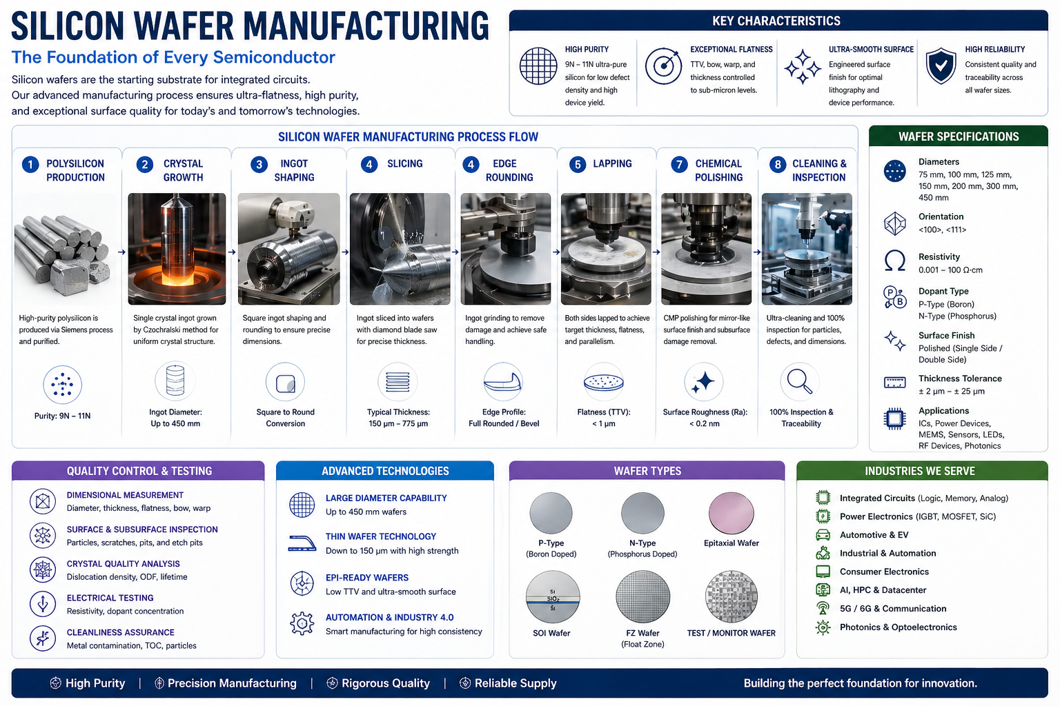
The silicon market is not a monolith; it is a highly segmented landscape where different grades of material are destined for vastly different technological futures. The Silicon Wafer Manufacturing Market segment for logic and memory devices represents the "high-end" of the market, where the focus is on 300mm wafers with the lowest possible defect density to support the smallest transistor sizes. In contrast, the market for discrete power devices and analog sensors often utilizes 200mm or even 150mm wafers. These "legacy" sizes remain highly profitable because the equipment for processing them is fully depreciated, and the technical requirements, while strict, do not require the same atomic-level precision as a leading-edge processor. This dual-track market allows manufacturers to maintain a balanced portfolio, serving both the cutting-edge tech giants and the stable industrial and automotive sectors.
We are also seeing the emergence of a specialized segment for "Photonics" and "Quantum" substrates. These wafers are designed to integrate optical components or superconducting qubits directly with electronic circuits. This requires unique dopant profiles and surface treatments that are quite different from traditional CMOS (Complementary Metal-Oxide-Semiconductor) wafers. As we transition toward a more data-centric world, the ability to move information using light instead of electricity is becoming a major priority, driving demand for wafers that can support high-speed laser and modulator integration. By understanding these diverse segments, substrate producers can better tailor their R&D investments and production capacity to match the evolving needs of the global tech industry. The future of silicon is one of increasing specialization, where the "blank slate" of the wafer is increasingly pre-engineered for its final destination.
FAQs
-
Why are 200mm wafers still used if 300mm are better? Many chips, like those for simple sensors or car power systems, don't need the extreme density of 300mm; using 200mm is much cheaper because the older factories are already paid for.
-
What is CMOS? It stands for Complementary Metal-Oxide-Semiconductor, which is the standard technology used to build nearly all of today’s integrated circuits and microprocessors.