

Gan On Si Epi Wafers Market: The Future of High-Efficiency Semiconductor Substrates
The global Gan On Si Epi Wafers Market is currently undergoing a transformative phase as the demand for high-performance power electronics reaches an all-time high. By utilizing Gallium Nitride (GaN) grown on traditional silicon substrates, manufacturers are able to bridge the gap between high-cost specialized materials and mass-market scalability. These gallium nitride silicon wafers offer a compelling combination of superior thermal conductivity and high breakdown voltage, making them indispensable for the next generation of power conversion systems. As industries move away from legacy silicon-only solutions, GaN epitaxial wafers are emerging as the gold standard for efficiency and compactness.
Market Overview and Introduction
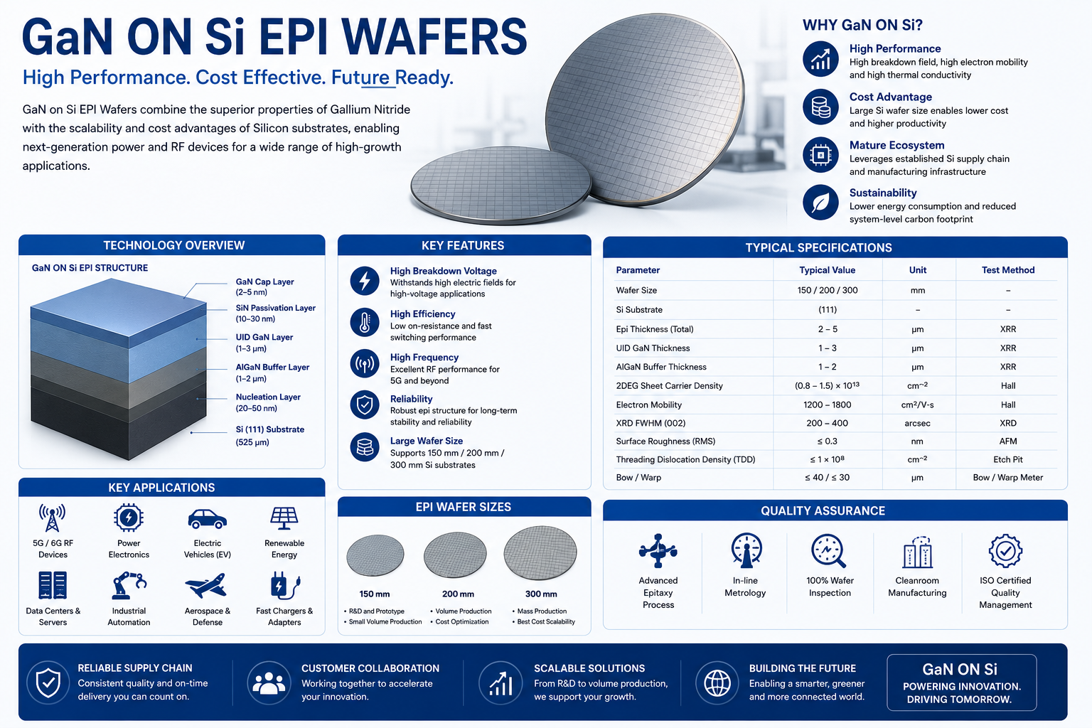
The emergence of GaN-on-Si technology represents one of the most significant leaps in semiconductor manufacturing in decades. Historically, power devices relied on pure silicon, which has physical limits regarding heat and frequency. GaN-on-Si allows for the deposition of a thin layer of Gallium Nitride on a silicon base, providing the performance of wide bandgap materials at a fraction of the cost of GaN-on-Sapphire or GaN-on-SiC. This has opened doors for various applications, ranging from 5G infrastructure to fast-charging consumer electronics.
Key Growth Drivers
Several factors are propelling this market forward. The primary driver is the rapid expansion of the electric vehicle (EV) sector. EVs require highly efficient on-board chargers and DC-DC converters to maximize battery range and reduce charging times. Additionally, the proliferation of 5G technology necessitates power amplifiers that can handle high frequencies with minimal energy loss. The inherent ability of these wafers to operate at higher temperatures and voltages compared to traditional silicon makes them the ideal candidate for these demanding environments.
Consumer Behavior and E-commerce Influence
In the semiconductor industry, consumer behavior is often reflected in the demand for smaller, faster, and more efficient electronic devices. Today's consumers expect ultra-fast charging for smartphones and laptops, which has led to a massive surge in GaN-based power adapters. Interestingly, e-commerce has influenced this market by accelerating the distribution of high-end components. B2B e-commerce platforms now allow smaller engineering firms to source semiconductor epi wafers and related components more easily, fostering innovation at the startup level and reducing the time-to-market for new consumer gadgets.
Regional Insights and Preferences
Asia-Pacific remains the dominant region in this market, driven by the massive semiconductor manufacturing hubs in Taiwan, China, and South Korea. These nations have invested heavily in infrastructure to support epitaxial growth processes. Meanwhile, North America and Europe are seeing significant growth in the automotive and aerospace sectors. In the United States, there is a strong preference for localized supply chains to mitigate global disruptions, leading to increased investment in domestic wide bandgap semiconductor materials production.
Technological Innovations and Emerging Trends
Innovation in this field is currently focused on increasing wafer diameters. Moving from 6-inch to 8-inch (200mm) silicon substrates is a major trend, as it significantly reduces the cost per die. Furthermore, improvements in MOCVD (Metal-Organic Chemical Vapor Deposition) technology are allowing for more uniform epitaxial layers with fewer defects. Emerging trends also include the integration of GaN devices directly onto CMOS logic circuits, creating "smart" power systems that can self-regulate and communicate status in real-time.
Sustainability and Eco-friendly Practices
Sustainability is a core component of the GaN value proposition. Because these materials allow for much higher energy efficiency in power conversion, they directly contribute to lower global energy consumption. In data centers, for instance, switching to GaN-based power supplies can save megawatts of electricity annually. Moreover, manufacturers are increasingly looking at "green" manufacturing processes, reducing the use of hazardous chemicals during the etching and deposition phases of wafer production.
Challenges, Competition, and Risks
Despite the benefits, the market faces hurdles. Lattice mismatch between Gallium Nitride and Silicon can cause mechanical stress and defects in the epi-layer, which impacts yield rates. Competition is also fierce; while GaN-on-Si is cost-effective, SiC (Silicon Carbide) remains a strong competitor in very high-voltage applications like heavy-duty industrial motors. Intellectual property disputes and the high cost of specialized deposition equipment also represent significant risks for new entrants.
Future Outlook and Investment Opportunities
The future of the industry looks exceptionally bright. As the world moves toward a "green" economy, the demand for power-efficient semiconductors will only grow. Investment opportunities are particularly strong in the development of 8-inch wafer processing facilities and specialized testing equipment for high-frequency GaN devices. As the technology matures and yields improve, we expect to see GaN-on-Si becoming the dominant substrate for almost all power applications under 1000V.